Materials Business
ACF – Anisotropic Conductive Film
  • ACF is suitable for creating electronic interconnections using conductive particles dispersed in adhesive.
  • It achieves electrical conductivity in the vertical direction at a certain temperature and pressure while requiring insulation between neighboring circuits and providing good adhesion.
Structure & Bonding Mechanism
LED-Chip on Glass image
Core Technology
NFA (Non-Flow ACF) Technology
NFA image
NFA image
Application
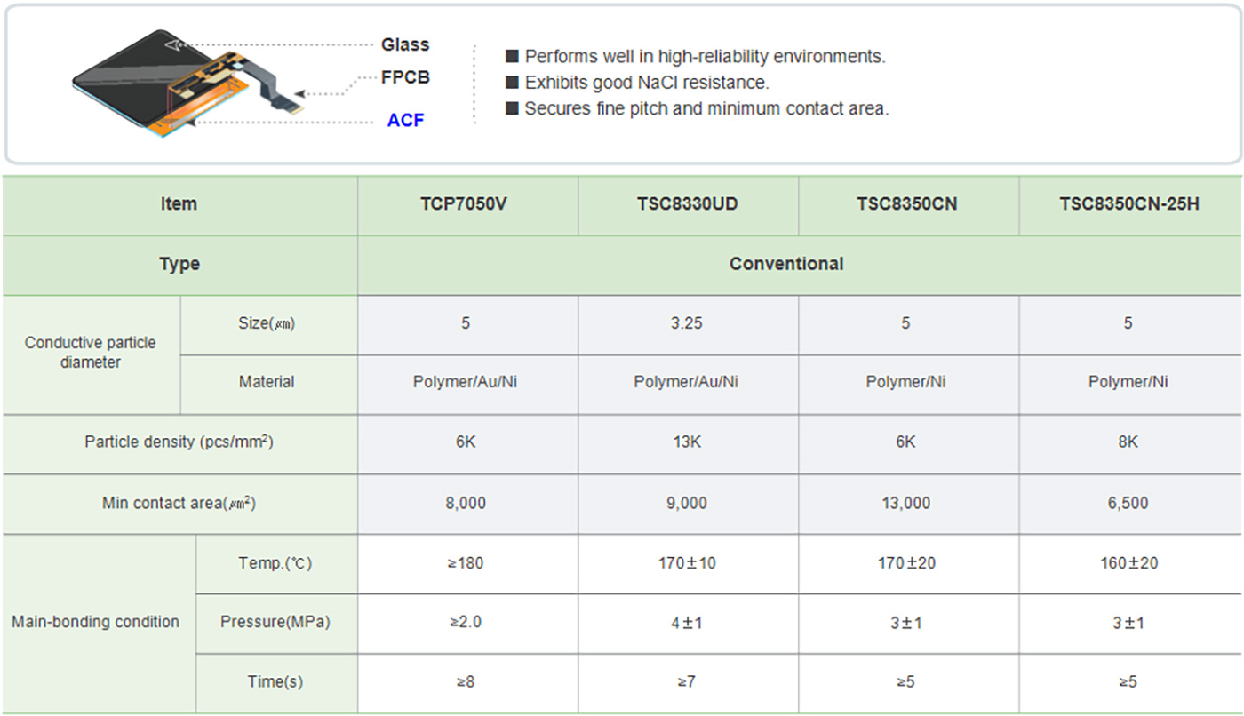
Fine-pitch electrodes in OLB, COG, COP, etc. → Prevents open-circuit and fine-pitch short-circuit defects
NFA table
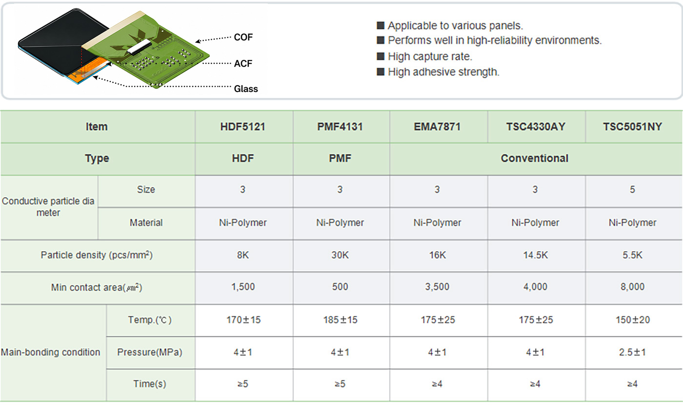
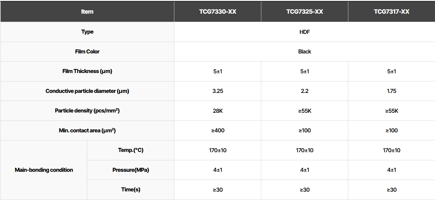
HDF (Hyper Distribution ACF) Technology
HDF image
HDF table
Application
Fine-pitch electrodes in OLB, COG, COP, μ-LED, and camera modules, etc.
→ Prevents open-circuit and fine-pitch short-circuit defects.
HDF table
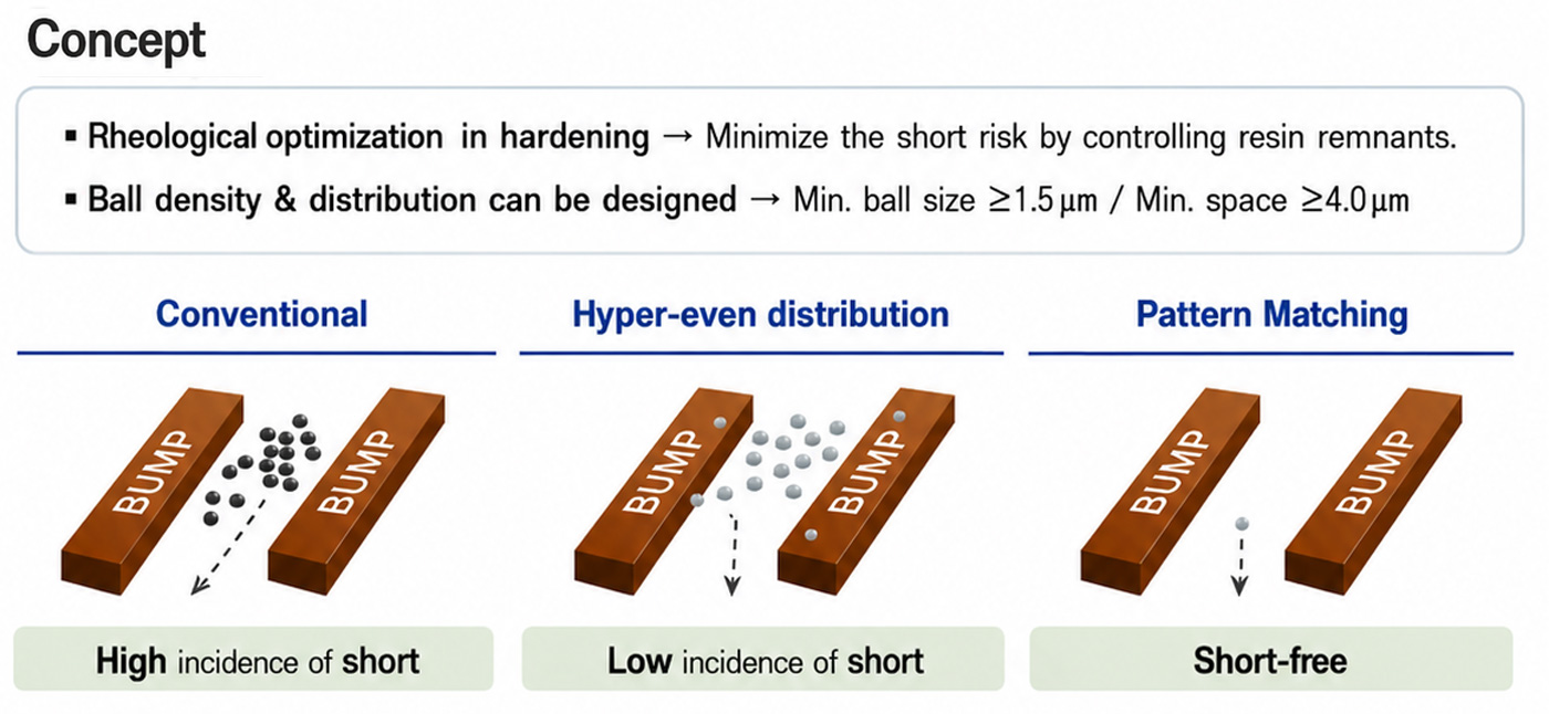
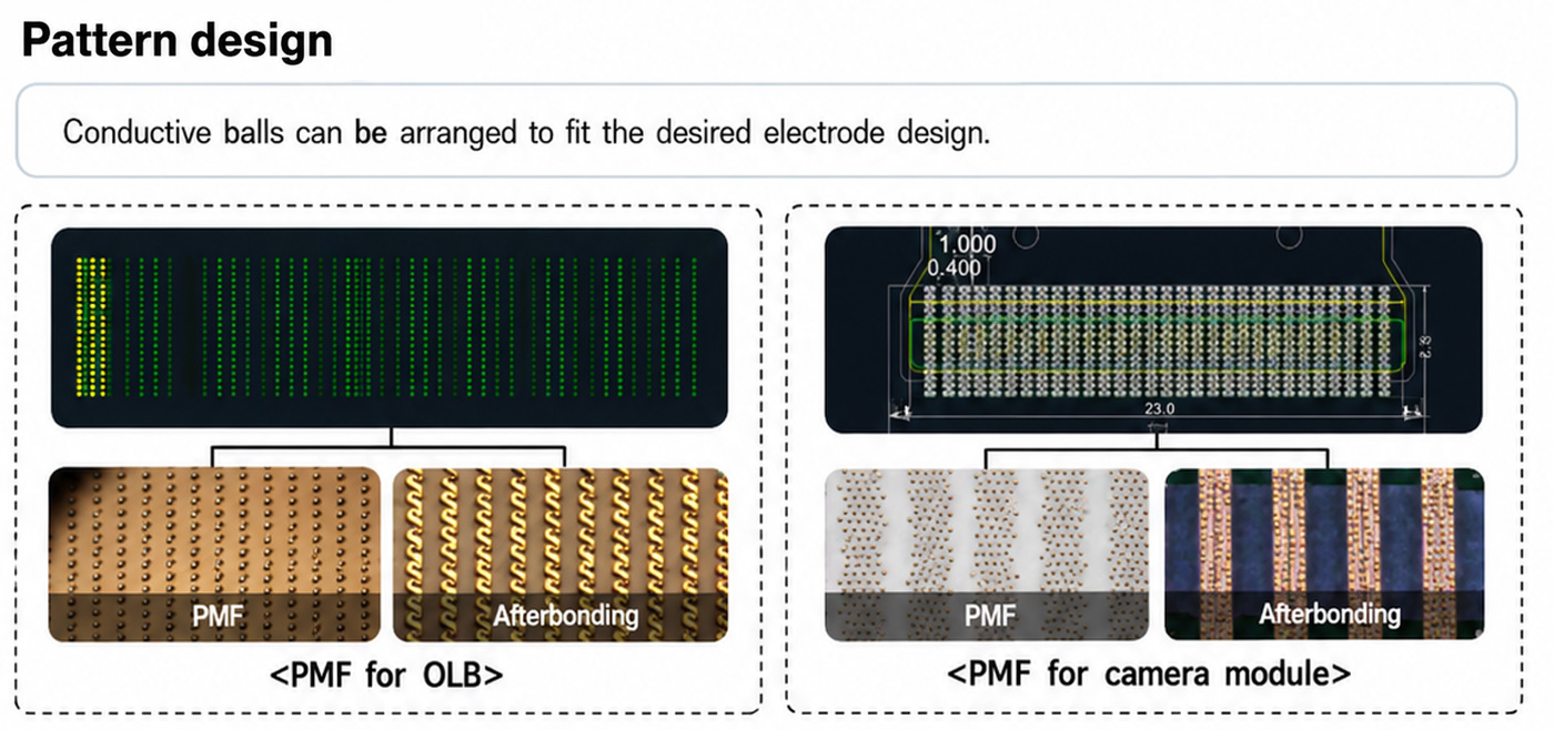
PMF (Pattern Matching Film) Technology
PMF image
PMF table
Application
Ultra-fine-pitch electrodes in OLB, COG, COP, and camera modules, etc.
→ Prevents open-circuit and fine-pitch short-circuit defects.
PMF table
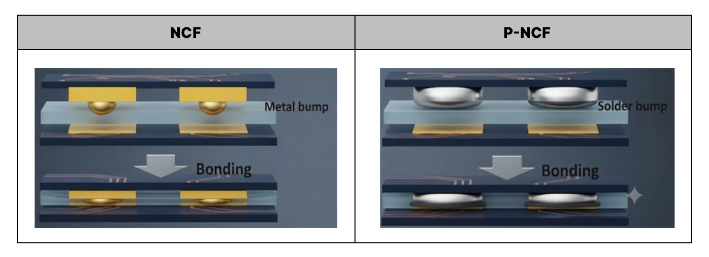
1. Definition
  • High-performance thermosetting adhesive film containing no conductive particles
  • Adhesive film optimized for fine-pitch and solder-bump bonding
  • Compatible with thermal compression (TC) bonding processes completed within 10 seconds, while providing excellent thermal curing performance
2. Key Applications
  • Packaging and interconnection of solder bumps and metal bumps
  • Fine-pitch circuit interconnection for semiconductor and display modules, including flip-chip bonding, IC packaging, and chip-on-film (COF) applications
  • Reliable electrical interconnection between metal pads made of gold (Au), nickel (Ni), copper (Cu), ITO, and other conductive materials
3. Key Technical Advantages
  • Excellent Adhesion: Provides strong interfacial adhesion and minimizes interfacial delamination
  • Precise Flow Control: Controls melt viscosity to prevent bump short-circuit and open-circuit defects
ncf image
1. Definition
  • Insulating film for fine-circuit formation
    : An inorganic-filler-loaded epoxy resin film used to build up fine-pattern circuit layers on a core substrate when processing large-area semiconductor package substrates (FC-BGA) for high-performance CPUs, GPUs, and similar devices
  • Main components: A blend of curable epoxy resin, curing agent, and nano-sized silica (SiO2) inorganic filler
2. Key Applications
  • High-performance semiconductor package substrates (FC-BGA/FC-CSP)
    : Fine interlayer insulation for interposers and package substrates that connect the main die to the mainboard in AI accelerators, server CPUs, high-performance GPUs, autonomous-driving APs, and more
  • High-density multilayer build-up substrates (HDI)
    : Fine-circuit build-up processes for compact, highly integrated boards such as smartphone mainboards and network switches
3. Key Technical Advantages
  • Ultra-fine line and space (L/S)
  • Low coefficient of thermal expansion (Low CTE)
  • Excellent insulation reliability and high-frequency performance: low dielectric constant and low dielectric loss
  • Strong plating adhesion and controlled surface roughness
Build up film image
1. Definition
  • Ultra-low-loss substrate bonding material – minimizing transmission loss in 5G ultra-high-frequency bands
  • High-performance thermosetting/thermoplastic adhesive film with controlled polar groups in its molecular structure
2. Key Applications
  • 5G mmWave antenna cables: interlayer bonding of high-speed transmission lines (MPI/LCP-based FPCBs) in the 10–40 GHz band
  • Multilayer FPCB lamination and insulation: coverlay for preventing crosstalk and protecting circuits in high-density multilayer boards
  • Next-generation interconnects: flexible cables for high-speed data transmission modules (USB4, PCIe Gen5/6, Thunderbolt)
3. Key Technical Advantages
  • Excellent high-frequency dielectric properties
    Dielectric constant (Dk) of 2.2–2.5 and dissipation factor (Df) of 0.0015–0.003 at 10 GHz, minimizing signal loss
  • High-temperature reflow resistance
Bonding Sheet image
ACF
(Anisotropic Conductive Film)
ACF is an insulating adhesive film in which fine conductive balls or particles are dispersed. When heat and pressure are applied, the conductive particles trapped between opposing electrodes establish electrical conduction in the vertical, or Z-axis, direction while maintaining insulation in the horizontal, or X-Y plane. This anisotropic conductivity enables fine-pitch circuits to be interconnected without electrical shorting between adjacent electrodes.

H&S HighTech’s ACF is a key electronic material that provides both electrical interconnection and mechanical bonding for fine-electrode components used in display panels, camera modules, flexible printed circuit boards (FPCBs), and chip-on-film (COF) packages. This is achieved by uniformly dispersing and arranging fine conductive particles within an insulating adhesive film. Leveraging its conductive-particle alignment and ultra-uniform distribution technologies, H&S HighTech is developing a portfolio of high-performance ACF products designed for next-generation interconnection applications, including fine-pitch assemblies, high-resolution displays, and MicroLED devices.
ACF image
OLB : COF on Glass
OLB image
Application
TV, MNT(LCD display, OLED display, high-resolution display, fine pitch, narrow bezel display) Laptop, Tablet, Mobile, Signage, ESL…
FOB : FPC/COF on Board
FOB image
Application
TV,Monitor, N-PC, Tablet, Mobile, Signage…
COG : Chip on Glass
COG image
Application
OLED display, Foldable display, Laptop, Tablet, Mobile, ESL …
FOG : FPCB on Glass
FOG image
Application
Fingerprint recognition sensor, OLED Mobile display, Automotive display, Laptop, Tablet, ESL …
COP : Chip on Plastic
COP image
Application
Mobile OLED display, Foldable OLED display…
FOP(S) : Film on Plastic / Si-wafer
FOP image
Application
AR/VR, Mobile OLED display, Foldable OLED display…
CM : Camera Module
Camera module image
Application
Mobile, Automotive...
MicroLED
MicroLED is a next-generation display technology that creates images using microscopic light-emitting diodes (LEDs).
Each pixel emits its own light, enabling high brightness and outstanding color reproduction.

MicroLED displays offer a high contrast ratio, fast response time, low power consumption, and long operational life, providing superior performance compared with conventional display technologies.
They are also highly resistant to burn-in and offer excellent durability, ensuring stable image quality across a wide range of operating environments.

Owing to these advantages, MicroLED is gaining significant attention as a key technology for advanced display applications, including large-format displays, next-generation TVs, wearable devices, and augmented reality/virtual reality (AR/VR) systems.
Micro-LED image

LED-Chip on Glass
  • An ACF for microLED connection. In mass production for chip sizes ranging from 20 to 100 µm
Micro LED image
Micro LED image
Application
Micro-LED TV, Automotive, AR, VR,MR, etc
Others image
Application
EV battery, Harness, Semiconductor packaging
FOF & Digitizer : FPCB on FPCB
FOF image
Application
Mobile, Tablet, Digitizer…
TOUCH : FPCB on PI/PET
Touch image
Application
Touch Film…
ncf image
Build up film table
Bonding Sheet table
Close